ADC HighSpeed SAR dsPIC - High-Speed SAR ADC for dsPIC33C

Overview
The MCHP_ADC_HighSpeed_SAR_dsPIC block configures the high-speed SAR (Successive Approximation Register) ADC peripheral found in dsPIC33CH and dsPIC33CK devices. This ADC architecture features 3-6 dedicated ADC cores (chip-dependent) plus one shared ADC7 core, enabling simultaneous multi-channel acquisition with independent trigger sources and conversion settings per core.
Block Variants
Two blocks configure the same hardware with different parameter organization:
- MCHP_ADC_HighSpeed_SAR_dsPIC (this block) - dsPIC-style interface with per-core tabs
- MCHP_ADC_HighSpeed_SAR - PIC32-style interface with channel arrays
Both blocks target the same peripheral.
Key Features
- 3-6 dedicated ADC cores (ADC0-ADC6, chip-dependent) with hard-wired analog inputs
- Shared ADC7 core for auxiliary channels (software multiplexing)
- 6/8/10/12-bit resolution selectable per core
- Up to 2.7 MSPS (shared core) / 3.7 MSPS (dedicated core) conversion rate (datasheet AD51 typ)
- Independent triggers per core (PWM, Timer, External Pin, Software)
- Hardware oversampling/filtering with sum or average modes (2-256 samples)
- DMA support for ping-pong buffering on dedicated cores
- Signed/unsigned output format selectable per core
- Fractional or integer output format (left or right aligned)
- PWM-synchronized acquisition for motor control current sensing
- Auxiliary clock option for optimized conversion speed
Block Dialog
The block dialog has 9 tabs: one main configuration tab, one tab per dedicated core (ADC0-ADC6), and one shared ADC tab. Tabs for non-existent cores are automatically hidden based on the selected chip.
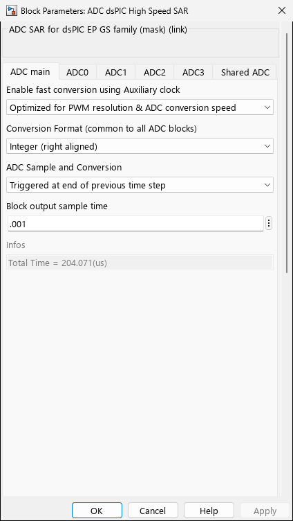
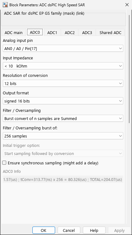
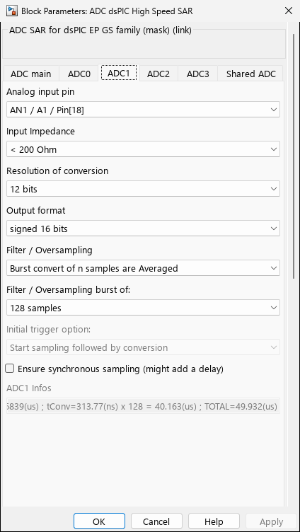
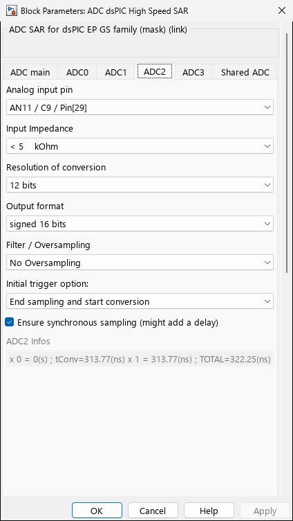
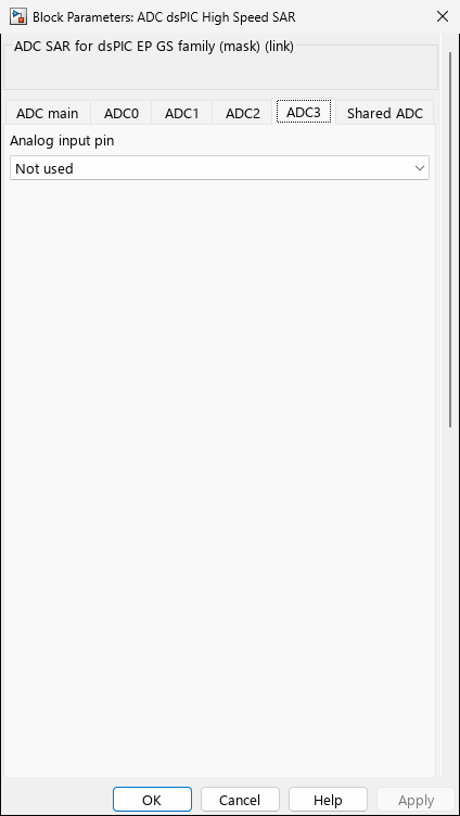
33EP64GS808Global ADC settings shared across all cores.
Per-core configuration tabs. Only tabs for existing cores are visible.
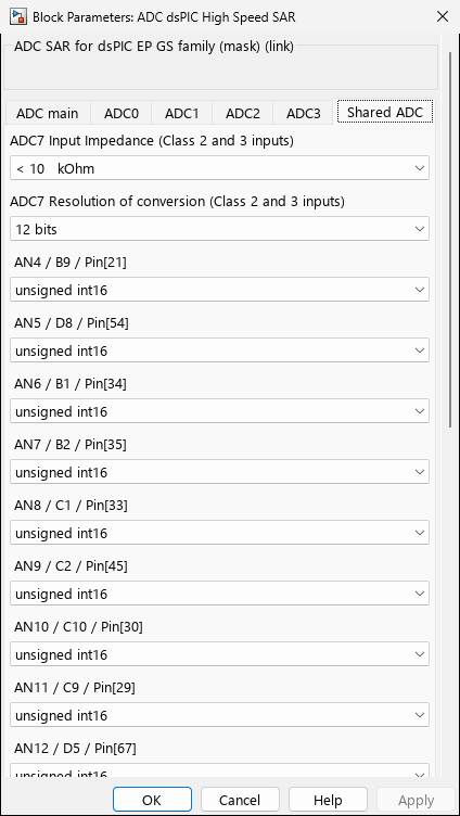
Tab 9: Shared ADC
Shared ADC7 configuration with checkbox selection for auxiliary analog inputs.
Ports
Input Ports
None. The ADC is triggered by hardware events (PWM, Timer) or software trigger, configured via block parameters.
Output Ports
Dynamic outputs created based on enabled ADC cores and selected analog inputs. Each enabled core or shared ADC input creates one output port.
Dedicated Core Outputs
Each enabled dedicated core creates one output port named after its analog input:
| Core | Typical Output Name | Description |
|---|---|---|
| ADC0 | AN0, ANA0, ANB0, ANC0 | Dedicated core 0 output |
| ADC1 | AN1, ANA1, ANB1, ANC1 | Dedicated core 1 output |
| ADC2 | AN2, ANA2, ANB2, ANC2 | Dedicated core 2 output |
| … | … | Additional cores as available |
The exact name depends on:
- Selected analog input (AN0, ANA0, ANB0, ANC0, PGA1, Vref_BanGap, etc.)
- Device-specific channel options
Shared ADC7 Outputs
Each selected analog input on shared ADC7 creates one output port named after the input:
- Standard inputs: AN7, AN8, AN9, … (varies by device)
- Special inputs: Temperature, Band Gap 1.2V, SPGA1, SPGA2, SPGA3, Vcore (chip-dependent)
DMA Vector Outputs
When DMA mode is enabled for dedicated cores (ADC0-6), outputs become vectors instead of scalars:
| DMA Mode | Output Size | Description |
|---|---|---|
| Single trigger | 1 element | Standard scalar output |
| 1 trig / 1 element | 1 element | Ping-pong buffer with one element |
| 2 trig / 2 elements | 2 elements | Ping-pong buffer |
| 3 trig / 3 elements | 3 elements | Ping-pong buffer |
| 4 trig / 4 elements | 4 elements | Ping-pong buffer |
Example: With ADC0 enabled and “2 trig / 2 elements” DMA mode, the output is a [1x2] vector containing two consecutive ADC samples.
Parameters
Global Parameters (ADC Main Tab)
Enable fast conversion using Auxiliary clock
Type: Popup
Default: “Optimized for PWM resolution & ADC conversion speed”
Options:
- Not used
- Optimized for PWM resolution & ADC conversion speed
- Optimized for PWM accuracy
Enables the auxiliary PLL (APLL) to generate a faster ADC clock independent of the PWM clock. This allows optimizing ADC speed without affecting PWM resolution.
When to use:
- “Optimized for PWM resolution & ADC conversion speed” - Use when you need both high PWM resolution (high PWM frequency) and fast ADC conversions. The APLL provides a faster ADC clock.
- “Optimized for PWM accuracy” - Use when PWM accuracy is critical and ADC speed is less important. ADC clock derived from system clock.
- “Not used” - Auxiliary clock disabled, ADC uses system-derived clock only.
Conversion Format (common to all ADC blocks)
Type: Popup
Default: “Integer (right aligned)”
Options:
- Integer (right aligned)
- Fractional (left aligned)
Controls the ADCON1Hbits.FORM register bit.
Integer format (FORM=0):
- 12-bit result right-aligned: bits [11:0] contain data, bits [15:12] = 0
- Example: 0x0FFF for full scale
Fractional format (FORM=1):
- Result left-aligned for Q15 fractional arithmetic
- 12-bit result: bits [15:4] contain data, bits [3:0] = 0
- Example: 0xFFF0 for full scale
Noise Reduction Enabled (might add delays)
Type: Checkbox
Default: Off
Visibility: Hidden (not available on most dsPIC33C devices)
Enables the ADCON1Lbits.NRE bit for noise reduction. This feature is only available on dsPIC33EP GS devices. The checkbox is hidden on dsPIC33CH/CK.
Multiple trigger - Vector output - for ADC[0-6] of current block
Type: Popup
Default: “Single trigger - (default)”
Options:
- Single trigger - (default)
- 1 trig / 1 element output (ping pong buffer)
- 2 trig / 2 elements output (ping-pong buffer)
- 3 trig / 3 elements output (ping-pong buffer)
- 4 trig / 4 elements output (ping-pong buffer)
Enables DMA-based buffering for dedicated cores (ADC0-6 only, not available for shared ADC7). When enabled, the block output becomes a vector containing multiple samples captured on consecutive triggers.
How it works:
- Each trigger captures one sample into a DMA buffer
- After N triggers, the block outputs a vector of N samples
- DMA uses ping-pong buffering: while one buffer fills, the previous buffer is read by Simulink
Example: “2 trig / 2 elements” with ADC0 enabled and PWM trigger:
- PWM trigger 1: Sample captured → DMA buffer A[0]
- PWM trigger 2: Sample captured → DMA buffer A[1], Simulink reads buffer A → output =
[sample1, sample2] - PWM trigger 3: Sample captured → DMA buffer B[0]
- PWM trigger 4: Sample captured → DMA buffer B[1], Simulink reads buffer B → output =
[sample3, sample4]
Limitations:
- Only for dedicated cores ADC0-6 (not shared ADC7)
- All enabled dedicated cores in this block share the same DMA buffer size
- Maximum buffer size: 4 elements
ADC Sample and Conversion
Type: Popup
Default: “Triggered at end of previous time step”
Options:
- Triggered at end of previous time step
- Triggered by custom source
- Continuously triggered. Output is last conversion
Determines how ADC conversions are triggered and synchronized with the Simulink model time step.
“Triggered at end of previous time step” (Timer-synchronized):
- ADC trigger comes from the master timer that drives the model time step
- Conversions occur synchronously with the Simulink scheduler
- Use for: Synchronized control loops, deterministic sampling
“Triggered by custom source” (User-defined trigger):
- ADC trigger comes from a user-selected source (PWM, Timer, External Pin)
- Allows independent triggering for each core
- Use for: PWM-synchronized motor control, event-driven acquisition
“Continuously triggered. Output is last conversion” (Free-running):
- ADC continuously converts using a global software trigger (GLSWTRG)
- Block output is the most recent conversion result
- Use for: Monitoring applications, non-synchronized measurements
User defined trigger
Type: Popup
Default: “Dynamic Options” (device-dependent)
Visibility: Visible when “Triggered by custom source” selected
Selects the trigger source for ADC conversions. The list is dynamically populated based on the selected chip.
Common trigger sources:
- PWM1 Trigger 1, PWM1 Trigger 2, PWM2 Trigger 1, … (PWM generators)
- SCCP1 Trigger, SCCP2 Trigger, … (CCP/SCCP timers)
- Timer1 period match, Timer2 period match (Timers - on dsPIC33CH)
- CLC1, CLC2 (Configurable Logic Cell outputs)
- PTG (Programmable Trigger Generator)
- ADTRG31 (PPS input) (External pin trigger via PPS)
For ADTRG31 (PPS input): On dsPIC33CK devices, when “ADTRG31 (PPS input)” is selected, a second popup appears to select the physical pin to map to the ADCTRG PPS input. The block automatically configures the PPS routing.
Example: Select “PWM1 Trigger 1” to trigger ADC conversions at a specific point in the PWM cycle (e.g., center-aligned PWM for motor control current sensing).
Synchronisation with model Time Step
Type: Popup
Default: “Trig model step after all sample using this trigger are converted”
Options:
- None (independant)
- Trig model step after all sample using this trigger are converted
- Trig model step after all sample from this block are converted
Controls when the Simulink model advances to the next time step relative to ADC conversion completion.
“None (independant)”:
- ADC conversions run independently of model time step
- Model does not wait for ADC to complete
- Use when ADC timing is not critical to control loop
“Trig model step after all sample using this trigger are converted”:
- Model waits for ALL ADC channels across ALL blocks that use the same trigger to complete
- Ensures all synchronized measurements are available before control algorithm runs
- Use for: Multi-block ADC configurations sharing a common trigger
“Trig model step after all sample from this block are converted”:
- Model waits only for conversions from THIS block to complete
- Other blocks with different triggers or other ADC blocks are ignored
- Use for: Single-block ADC configurations or when this block’s measurements are critical
How it works internally: The block determines the slowest ADC channel (longest conversion time) and configures an interrupt on that channel’s completion to trigger the Simulink task. For dedicated cores (ADC0-6), the slowest core triggers. For shared ADC7, the last sequential channel triggers.
Block output sample time
Type: Edit
Default: 0.001 (1 ms)
Simulink sample time for the block’s output ports. Set to match your control loop period.
Typical values:
- 0.0001 (100 µs) - Fast current control loops
- 0.001 (1 ms) - Velocity control, general motor control
- -1 - Inherited sample time
Dedicated Core Parameters (ADC0-ADC6 Tabs)
Each dedicated core has its own configuration tab with the following parameters:
Analog input pin
Type: Popup
Default: “Dynamic Options” (device-dependent)
Options:
- Not used
- AN0 / A0 / Pin[21] (example)
- ANA0 / A0 / Pin[21] (alternate)
- PGA1 (programmable gain amplifier input)
- Vref_BanGap (internal band gap reference)
- … (device-specific)
Selects the analog input source for this dedicated core. The list is populated based on the chip’s datasheet and includes:
- Standard analog inputs (AN0, AN1, …)
- Alternate inputs (ANA0, ANB0, ANC0 on devices with input multiplexing)
- Internal sources (PGA, band gap reference)
Pin mapping:
The popup displays the pin assignment: ANx / Port / Pin[number]
- ANx - Analog input number
- Port - GPIO port (A0, B4, etc.)
- Pin[number] - Physical pin number on the package
Hardware limitation: Each dedicated core is hard-wired to specific analog input options defined by the chip architecture. You cannot arbitrarily assign any ANx to any core. Check the device datasheet for core-to-input mapping.
“Not used”: Select this to disable the core. No output port is created.
Input Impedance
Type: Popup
Default: “< 10 kOhm”
Options:
- < 200 Ohm
- < 500 Ohm
- < 1 kOhm
- < 2 kOhm
- < 5 kOhm
- < 10 kOhm
- < 20 kOhm
- < 50 kOhm
- < 100 kOhm
- < 200 kOhm
- < 500 kOhm
- max sampling time
Specifies the maximum source impedance connected to this analog input. The block automatically calculates the minimum required sampling time (SAMC) based on this impedance to ensure accurate conversions.
Impedance-to-sampling time formula: @@PROT_1@@
Examples:
- < 200 Ω → SAMC ≥ 3 TAD
- < 10 kΩ → SAMC ≥ 23 TAD
- < 100 kΩ → SAMC ≥ 203 TAD
“max sampling time”: Select this to use the maximum SAMC value (1023 TAD), allowing accurate conversion of very high impedance sources (e.g., resistive dividers with hundreds of kΩ).
Where SAMC is used:
- For dedicated cores (ADC0-6): @@PROT_30@@ (if SAMCEN not set)
- For shared ADC7: @@PROT_31@@
Info field: The “ADCx Info” read-only field at the bottom of each tab displays the calculated timing: @@PROT_2@@
Resolution of conversion
Type: Popup
Default: “12 bits”
Options:
- 6 bits
- 8 bits
- 10 bits
- 12 bits
Sets the ADC resolution for this core via the @@PROT_32@@ field (SELRESx register).
| Resolution | Max Value | Conversion Time (typical) | Use Case |
|---|---|---|---|
| 12 bits | 4095 (0xFFF) | ~272 ns × 12 = 3.3 µs | High precision measurements |
| 10 bits | 1023 (0x3FF) | ~272 ns × 10 = 2.7 µs | Moderate precision, faster |
| 8 bits | 255 (0xFF) | ~272 ns × 8 = 2.2 µs | Fast conversions |
| 6 bits | 63 (0x3F) | ~272 ns × 6 = 1.6 µs | Maximum speed |
Trade-off: Higher resolution → more accurate → slower conversion. Lower resolution → less accurate → faster conversion.
Output format
Type: Popup
Default: “signed 16 bits”
Options:
- unsigned 16 bits
- signed 16 bits
Determines the output data type and the sign configuration for this core.
“unsigned 16 bits”:
- Simulink output data type: @@PROT_33@@
- @@PROT_34@@ (unsigned mode)
- Input voltage range: 0 to VREF
- Raw output range: 0 to (2^resolution - 1)
“signed 16 bits”:
- Simulink output data type: @@PROT_35@@
- @@PROT_36@@ (signed mode)
- Input voltage range: -VREF to +VREF (differential or bipolar mode)
- Raw output range: -(2^(resolution-1)) to +(2^(resolution-1) - 1)
Typical usage:
- Unsigned: Single-ended measurements (voltage monitoring, temperature sensors)
- Signed: Differential measurements, bipolar signals, AC current sensing with offset
Filter / Oversampling
Type: Popup
Default: “No Oversampling”
Options:
- No Oversampling
- Burst convert of n samples are Summed
- Burst convert of n samples are Averaged
Enables hardware oversampling/filtering using the ADC’s built-in digital filter (ADCFLTRx register).
“No Oversampling”:
- Single conversion per trigger
- No filtering applied
- Fastest response
“Burst convert of n samples are Summed”:
- Captures multiple samples and returns their sum
- @@PROT_37@@ (Sum mode)
- Output range: 0 to (2^resolution - 1) × n_samples
- Use for: Noise reduction via accumulation, energy measurements
“Burst convert of n samples are Averaged”:
- Captures multiple samples and returns their average
- @@PROT_38@@ (Average mode)
- Output range: 0 to (2^resolution - 1) (same as single sample)
- Use for: Noise reduction, effective resolution increase via oversampling
When enabled, also configure: “Filter / Oversampling burst of” parameter.
Filter / Oversampling burst of
Type: Popup
Default: “256 samples”
Options:
- 2 samples
- 4 samples
- 8 samples
- 16 samples
- 32 samples
- 64 samples
- 128 samples
- 256 samples
Selects the number of samples (n) for burst oversampling when filtering is enabled.
Register configuration:
- @@PROT_39@@ field
- For Sum mode: @@PROT_40@@ using a lookup table
- For Average mode: @@PROT_41@@
Effective resolution increase (Average mode): Oversampling can increase effective resolution by reducing quantization noise: @@PROT_3@@
| Samples | Extra Bits | Effective Resolution (12-bit base) |
|---|---|---|
| 4 | 1 bit | 13 bits |
| 16 | 2 bits | 14 bits |
| 64 | 3 bits | 15 bits |
| 256 | 4 bits | 16 bits |
Conversion time impact: Total conversion time = (sampling time + conversion time) × n_samples
Example: 12-bit resolution, 256 sample average:
- Single conversion: 3.3 µs
- Burst of 256: 3.3 µs × 256 = 845 µs
Initial trigger option
Type: Popup
Default: “End sampling and start conversion”
Options:
- End sampling and start conversion
- Start sampling followed by conversion
Controls the behavior of the trigger event via the @@PROT_42@@ bit (STRGEN parameter).
“End sampling and start conversion” (SAMCEN = 0, default):
- Trigger event ends the sampling phase and immediately starts the conversion
- Sampling time is determined by when the previous conversion completed
- Use for: Standard triggered acquisition
“Start sampling followed by conversion” (SAMCEN = 1):
- Trigger event starts a new sampling phase for the time specified in SAMC
- After SAMC TAD cycles, conversion starts automatically
- Use for: Precise control of sampling timing, pre-synchronized sampling
Timing diagram:
@@PROT_4@@
Ensure synchronous sampling (might add a delay)
Type: Checkbox
Default: Off
Enables synchronous sampling mode via the @@PROT_43@@ bit (SSAMPEN parameter).
When enabled:
- Sampling is synchronized across multiple cores
- May introduce a delay to align sampling phases
- Use for: Phase-accurate multi-channel acquisition (e.g., three-phase motor currents)
When disabled:
- Each core samples independently as soon as triggered
- No synchronization delay
- Use for: Fastest possible conversions
Shared ADC7 Parameters (Shared ADC Tab)
The shared ADC7 core uses a software-controlled multiplexer to select from multiple analog inputs. Unlike dedicated cores, you enable individual inputs via checkboxes, and each enabled input creates a separate output port.
ADC7_ANx (Checkboxes for each available input)
Type: Popup per analog input
Default: “Not used”
Options:
- Not used
- unsigned int16
- signed int16
- unsigned int16 2 samples summed
- unsigned int16 4 samples summed
- … (up to 256 samples)
- unsigned int16 2 samples averaged
- unsigned int16 4 samples averaged
- … (up to 256 samples)
- signed int16 2 samples summed/averaged (similar options)
Each available analog input (typically AN7 and above) has its own popup. The popup combines multiple settings:
- Enable/disable (“Not used” disables)
- Output format (signed/unsigned)
- Data type (int16)
- Oversampling (none, summed, or averaged)
- Number of samples (2, 4, 8, … 256)
Example selections:
- “unsigned int16” - Single sample, unsigned, no filtering
- “unsigned int16 16 samples averaged” - 16 samples averaged, unsigned output
- “signed int16 64 samples summed” - 64 samples summed, signed output
Pin mapping: The prompt string displays the pin assignment: @@PROT_44@@ (example)
Special inputs: On some devices, shared ADC7 can access internal signals:
- Temperature sensor (chip-dependent)
- Band Gap 1.2V reference (chip-dependent)
- SPGA1/SPGA2/SPGA3 - Sigma-Delta PGA outputs (dsPIC33CH)
- Vcore - Core voltage (some devices)
The availability of these special inputs depends on the chip’s maskset and is detected from the chip database.
Input Impedance (ADC7)
Type: Popup
Default: “< 10 kOhm”
Options: Same as dedicated cores
Specifies the maximum source impedance for ALL inputs connected to shared ADC7. The block calculates the required SHRSAMC value for the shared core.
Resolution of conversion (ADC7)
Type: Popup
Default: “12 bits”
Options: 6/8/10/12 bits
Sets the resolution for shared ADC7. All inputs on shared ADC7 use the same resolution.
ADC Trigger Info (Read-only)
Displays calculated timing information for ADC7 conversions, including per-channel conversion times and total sequential conversion time.
ADC Timing Calculation
The block automatically calculates ADC timing parameters and displays them in the “Info” fields on each tab.
Timing Components
1. Sampling Time (tSample): @@PROT_5@@
- SAMC - Sample time in TAD cycles (calculated from input impedance)
- TAD - ADC clock period = 1 / fADC
2. Conversion Time (tConversion): @@PROT_6@@
- Resolution - 6, 8, 10, or 12 bits
- +2 - Additional cycles for acquisition and conversion settling
3. Total Conversion Time: @@PROT_7@@
4. For Oversampling: @@PROT_8@@
5. For Shared ADC7 (sequential channels): @@PROT_9@@
Example Calculation
Configuration:
- Input impedance: < 10 kΩ
- Resolution: 12 bits
- fADC: 50 MHz (TAD = 20 ns)
Calculation:
- SAMC = 0.002 × 10000 + 3 = 23 TAD
- tSample = 23 × 20 ns = 460 ns
- tConversion = (12 + 2) × 20 ns = 280 ns
- tTotal = 460 + 280 = 740 ns
Displayed in Info field: @@PROT_10@@
Clock Configuration
The ADC clock (TAD) is derived from either the system clock or the auxiliary PLL:
System clock path: @@PROT_11@@
- CLKDIV configured in @@PROT_45@@
Auxiliary PLL path (if enabled): @@PROT_12@@
- APLL typically 400-800 MHz
- Enables faster conversions independent of PWM clock
The block automatically selects CLKDIV to maximize ADC speed while respecting the maximum fADC specification (typically 50 MHz).
Trigger Configuration
Trigger Sources by Device
The available trigger sources vary by device family:
dsPIC33CK
- PWM1-8 Trigger 1, Trigger 2
- SCCP1-8 Trigger / CCP Interrupt
- MCCP9 Trigger / CCP Interrupt
- CLC1-4 Output
- PTG (Programmable Trigger Generator)
- ADTRG31 (PPS input)
dsPIC33CH (Master/Slave)
Master core:
- Master PWM1-4 Trigger 1, Trigger 2
- Master SCCP1-4 input capture/output compare
- Slave PWM Trigger 2 (from slave core)
- Master CLC1, Slave CLC1
- Master PTG
- ADTRG31 (PPS input)
Slave core:
- Slave PWM1-8 Trigger 1, Trigger 2
- Slave SCCP1-8
- ADTRG31 (PPS input)
Trigger Synchronization Strategies
The block supports four synchronization strategies:
1. Free-Running (Continuous Trigger)
Configuration: “Continuously triggered. Output is last conversion”
Behavior:
- Global software trigger (GLSWTRG) continuously triggers all enabled cores
- Output is the most recent conversion result
- No synchronization with Simulink time step
Use case: Monitoring applications, non-critical measurements
2. Model Time Step Trigger
Configuration: “Triggered at end of previous time step”
Behavior:
- Master timer triggers ADC at end of each time step
- Model waits for ADC completion before advancing
- Deterministic sampling synchronized with control loop
Use case: Standard control loops, synchronized data acquisition
3. Custom Trigger (Independent)
Configuration: “Triggered by custom source” + “None (independant)”
Behavior:
- User-selected trigger (PWM, Timer, External Pin)
- ADC runs independently of Simulink time step
- Output updated asynchronously
Use case: Event-driven acquisition, PWM-synchronized measurements not critical to model timing
4. Custom Trigger (Synchronized)
Configuration: “Triggered by custom source” + “Trig model step after all sample…”
Behavior:
- User-selected trigger (typically PWM Special Event)
- Model waits for ADC completion before advancing
- Ensures measurements available before control algorithm executes
Use case: Motor control current sensing, PWM-synchronized control loops
PWM-Synchronized Motor Control
For motor control applications, the typical configuration is:
Setup:
- PWM block generates three-phase waveforms
- PWM Special Event Trigger configured at specific PWM phase (e.g., center-aligned)
- ADC block triggered by “PWMx Trigger 1”
- Synchronization: “Trig model step after all sample from this block are converted”
Timing: @@PROT_13@@
Benefits:
- Current measured at optimal point in PWM cycle (e.g., center for center-aligned PWM)
- Control algorithm runs with fresh current measurements
- Deterministic timing for stable control
Register Configuration (click to expand)
Register Configuration
The block configures the following dsPIC33C ADC registers:
Global Configuration
| Register | Bit Field | Description | Configured By |
|---|---|---|---|
| ADCON1H | FORM | Output format (0=integer, 1=fractional) | “Conversion Format” |
| ADCON1L | NRE | Noise reduction enable | “Noise Reduction Enabled” |
| ADCON5H | WARMTIME | Wake-up time (min 10 µs) | Auto-calculated |
| ADCON3H | CLKSEL | Clock source: 11=FVCO/4, 10=FVCO/3, 01=FOSC, 00=FCY (silicon-verified; the WAC0B/Andromeda+ datasheet erroneously swaps 01/00 — see Jira DS_WAC0B-68). The block emits only 01=FOSC or 11=aux PLL. | “Auxiliary clock” |
| ADCON3H | CLKDIV | Clock divider | Auto-calculated |
| ADCON3L | REFSEL | Reference source (0=AVdd/AVss) | Fixed to 0 |
Dedicated Core Configuration (ADC0-6)
| Register | Bit Field | Description | Configured By |
|---|---|---|---|
| ADCON4H | CxCHS | Core x channel select | “Analog input pin” |
| ADCORExL | SAMC | Sample time (TAD cycles) | “Input Impedance” |
| ADCORExH | RES | Resolution (0=6-bit, 1=8-bit, 2=10-bit, 3=12-bit) | “Resolution of conversion” |
| ADCON4L | SAMCxEN | Sample enable mode | “Initial trigger option” |
| ADCON4L | SYNCTRGx | Synchronous trigger | “Ensure synchronous sampling” |
Trigger Configuration
| Register | Bit Field | Description | Configured By |
|---|---|---|---|
| ADTRIGxL | TRGSRCx | Trigger source for core x | “User defined trigger” |
| ADTRIGxH | TRGSRCx | Trigger source (continued) | “User defined trigger” |
| ADLVLTRGL/H | LVLENx | Level trigger enable | Auto (based on trigger type) |
Filtering/Oversampling
| Register | Bit Field | Description | Configured By |
|---|---|---|---|
| ADCFLTRx | FLEN | Filter enable | “Filter / Oversampling” |
| ADCFLTRx | MODE | Filter mode (0=sum, 3=average) | “Filter / Oversampling” |
| ADCFLTRx | OVERSAM | Oversampling ratio | “Filter / Oversampling burst of” |
| ADCFLTRx | CHNLID | Channel ID (which input) | Auto (core index) |
Sign Configuration
| Register | Bit Field | Description | Configured By |
|---|---|---|---|
| ADCMPxCON1 | SIGNENx | Signed enable for input x | “Output format” |
DMA Configuration
| Register | Bit Field | Description | Configured By |
|---|---|---|---|
| ADCON1L | DMABL | DMA buffer length (log2) | “Multiple trigger - Vector output” |
Interrupt Configuration
The block automatically configures ADC interrupts when time step synchronization is enabled:
| Register | Bit Field | Description |
|---|---|---|
| ADIExL/H | IEx | Interrupt enable for core x |
| _IPCx | Priority | Interrupt priority (auto) |
The interrupt triggers the Simulink task when the last ADC channel completes conversion.
Scaling and Units
Raw ADC Value to Voltage
The block outputs raw ADC counts (unsigned or signed integer). To convert to voltage:
Integer Format (right-aligned)
Unsigned:
Voltage = (ADC_counts / ADC_max) × VREF
Signed:
Voltage = ((ADC_counts / ADC_max) × VREF × 2) - VREF
Where:
ADC_max= 2^resolution - 1 (e.g., 4095 for 12-bit)VREF= Reference voltage (typically 3.3V)
Fractional Format (left-aligned)
Unsigned Q15:
Voltage = (ADC_counts / 32768) × VREF
Signed Q15:
Voltage = (ADC_counts / 32768) × VREF
(Signed Q15 range: -1 to +0.9999)
Oversampling Output Scaling
When oversampling is enabled:
Sum mode:
- Output range: 0 to (ADC_max × n_samples)
- Voltage formula:
Voltage = (ADC_sum / (ADC_max × n_samples)) × VREF
Average mode:
- Output range: 0 to ADC_max (same as single sample)
- Voltage formula: Same as single sample
- Benefit: Improved effective resolution, reduced noise
Example Scaling Block Diagram
ADC Output (uint16) ──► Gain: VREF/ADC_max ──► Data Type: single ──► Voltage (V)
For 12-bit unsigned, VREF=3.3V:
ADC Output (uint16) ──► Gain: 3.3/4095 = 0.000806 ──► Voltage (V)
Code Generation Details (click to expand)
Code Generation
The TLC file (MCHP_ADC_HighSpeed_SAR_dsPIC.tlc) generates initialization code in the model’s Start function and interrupt service routines if time step synchronization is enabled.
Generated Code Structure
Initialization (Start function):
/* ADC common settings */
ADCON1Hbits.FORM = 0;               // Integer format
ADCON5Hbits.WARMTIME = 10;          // 10 µs warm-up
ADCON3Hbits.CLKSEL = 1;             // Auxiliary PLL
ADCON3Hbits.CLKDIV = 7;             // Clock divider
ADCON3Lbits.REFSEL = 0;             // AVdd/AVss reference

/* Dedicated core configuration */
ADCON4Hbits.C0CHS = 0;              // ADC0 -> AN0
ADCORE0L = 23;                      // Sampling time
ADCON4Lbits.SAMC0EN = 0;            // Trigger ends sampling

/* Trigger configuration */
ADTRIG0Lbits.TRGSRC0 = 4;           // PWM1 Trigger 1

/* Enable ADC */
ADCON1Lbits.ADON = 1;               // Turn on ADC
Interrupt Service Routine (if synchronized):
void __attribute__((__interrupt__, auto_psv)) _ADCAN0Interrupt(void)
{
    IFS5bits.ADCAN0IF = 0;          // Clear interrupt flag
    // Read ADC result
    // Trigger Simulink task
}
Integration with Simulink Scheduler
When “Trig model step after conversion” is enabled, the generated code uses the ADC interrupt to trigger the Simulink task, ensuring measurements are available before the control algorithm executes.
Device Support
This block targets dsPIC33C family devices:
dsPIC33CH (Dual-Core)
dsPIC33CH (Dual-Core)
Dual-core devices with master/slave architecture. Check device datasheet for exact ADC core count.
Example devices:
- dsPIC33CH512MP508 - Master and slave cores
dsPIC33CK (Single-Core)
dsPIC33CK (Single-Core)
Single-core high-performance DSCs with up to 6 dedicated ADC cores.
Example devices:
- dsPIC33CK64MC105
- dsPIC33CK256MP508
- dsPIC33CK512MP608
- dsPIC33CK1024MP710
dsPIC33CDV (Digital Power)
dsPIC33CDV (Digital Power)
Digital power devices with integrated voltage regulators.
Example devices:
- dsPIC33CDV64MC106
Number of Dedicated Cores by Device
The number of dedicated ADC cores varies by device. The block automatically detects available cores from the chip database (MCHP.ADC.HS_SAR.nDedicatedCore).
| Device Family | Typical Core Count | Notes |
|---|---|---|
| dsPIC33CK MP/MC | 4-6 cores | High pin count devices have more cores |
| dsPIC33CH | 3-6 cores | Varies by device |
| dsPIC33CDV | 3-4 cores | Digital power optimized |
Examples
Programmatic Setup
% Add block to model
add_block('MCHP_Blockset/Analog IO/ADC dsPIC\nHigh Speed SAR', [mdl '/ADC_HS']);

% Configure key parameters
set_param([mdl '/ADC_HS'], 'ADC0_pin', 'AN0');
set_param([mdl '/ADC_HS'], 'ADC0_R', '< 10   kOhm');
set_param([mdl '/ADC_HS'], 'ADC0_res', '12 bits');
References
- dsPIC33C Family Reference Manual - Section 37: High-Speed SAR ADC
- DS70005213 - dsPIC33CH/CK High-Speed ADC
- DS70005320 - dsPIC33C Electrical Characteristics
Related Blocks
ADC HighSpeed SAR - PIC32-style interface for the same hardware
ADC - Standard 10-bit ADC for dsPIC30F/33F/33E
PWM Blocks - PWM blocks for motor control trigger sources
PWM Category — ADC Synchronization — See “PWM-ADC Synchronization” section