Digital Output

Overview
The Digital Output block is a composite subsystem block that provides digital output functionality with optional read-back capability. This block automatically manages internal sub-blocks:
- Always present: Digital Output Write sub-block
- Optional: Digital Output Read sub-block (added when “Read previous value written” is enabled)
The block handles all internal connections and parameter propagation automatically. When the block input is defined as one uint16, the value is used as-is without masks, which may affect other pins on the same port if they are also configured as digital outputs.
When to use:
- Controlling LEDs, relays, or actuators
- Generating digital control signals
- Interfacing with digital peripherals
- When you need optional read-back of the output state
When NOT to use:
- For high-frequency PWM generation (use PWM blocks instead)
- When precise timing control is required (use Timer Output Compare instead)
Block Dialog
The Digital Output library entry has two variants — Write (set pin level from a Simulink input) and Read (read back the current pin level). Each has its own mask dialog.
Digital Output — Write
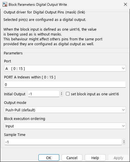
Screenshots taken with chip 33AK512MPS512
Digital Output — Read
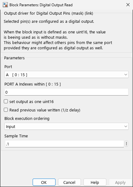
Screenshots taken with chip 33AK512MPS512
Ports
Input
| Port | Data Type | Description |
|---|---|---|
| Port signal | boolean or uint16 | Digital value to write to selected pin(s). If multiple pins are selected without PACK option, each pin requires its own boolean input. If PACK option is enabled, a single uint16 input sets multiple pins via bit positions. |
Output (Optional)
| Port | Data Type | Description |
|---|---|---|
| Port signal | boolean or uint16 | Current output state read from LAT register (1 sample delay). Only present when “Read previous value written (1/z delay)” is enabled. |
Parameters
| Parameter | Variable | Type | Description |
|---|---|---|---|
| Port | PORT | popup | GPIO port selection (A, B, C, etc.). Dynamically populated based on target device pin map. Shows available pin indices for each port. |
| Pins | PIN | edit | Array of pin indices to control, e.g., [0] or [0 1 2]. Valid range is [0..15] for 16-bit ports or [0..31] for 32-bit ports. Out-of-range or unavailable pins are automatically filtered out with a warning. Defaults to [0] if left empty. |
| Initial Output | INIT_VALUE | edit | Chip-dependent. Initial pin state at startup. Accepts scalar (applies to all pins), vector (per-pin values), or bitmask (when PACK enabled). Use -1 or any negative value for “don’t care” (leaves pin at reset state). Visible on dsPIC30F, dsPIC33F, dsPIC33E, dsPIC33C, dsPIC33A, PIC32, PIC32A (Arch 1,2,3,4,8). Hidden on SAM devices. |
| set input as one uint16/uint32 | PACK | checkbox | When enabled, accepts a single uint16 (16-bit ports) or uint32 (32-bit ports) input where bit positions correspond to pin numbers. Enables atomic multi-pin updates. |
| Request exact simultaneous write | SIMULTANEOUS | checkbox | Conditional. When enabled, all pins are written to LAT register in a single instruction for atomic simultaneous update. Only visible when multiple pins are selected AND PACK is disabled. |
| Output mode | OUTPUT_PIN_MODE | popup | Chip-dependent. Electrical configuration: Push-Pull (default) for standard CMOS output, or Open Drain for open-collector applications. Only visible on dsPIC33E, dsPIC33C, dsPIC33A, PIC32, PIC32A (Arch 3,4,8). Hidden on older dsPIC30F/33F and SAM devices. |
| Read previous value written (1/z delay) | READPREVIOUS | checkbox | Adds Digital Output Read sub-block and output port to read LAT register state with 1 sample delay. |
| Block execution ordering | ORDERING | popup | Controls block scheduling: None, Input, Output, or Input & Output. When READPREVIOUS is enabled, ordering is automatically managed across sub-blocks. |
| Sample Time | SampleTime | edit | Sampling interval in seconds. Use -1 for inherited sample time. |
Device Support
Initial Output Parameter Visibility:
- Visible: dsPIC30F, dsPIC33F, dsPIC33E, dsPIC33C, dsPIC33A, PIC32, PIC32A (Arch 1,2,3,4,8)
- Hidden: All SAM (SAME70/SAMS70/SAMV71/SAMx2/SAMx5) devices
- When hidden, pins start at hardware reset state (typically Hi-Z)
Output Mode Parameter Visibility:
- Visible (Push-Pull/Open Drain): dsPIC33E, dsPIC33C, dsPIC33A, PIC32, PIC32A (Arch 3,4,8)
- Hidden (Push-Pull only): dsPIC30F, dsPIC33F (Arch 1,2) and all SAM devices
- When hidden, pins use standard Push-Pull CMOS output mode
Sub-block Management:
- When
READPREVIOUS=off: Only Digital Output Write sub-block is present - When
READPREVIOUS=on: Both Digital Output Write and Digital Output Read sub-blocks are present, with internal ordering connection - Parameters (
PORT,PIN,PACK,SIMULTANEOUS,OUTPUT_PIN_MODE,INIT_VALUE,SampleTime) are automatically propagated to sub-blocks - Block ordering is automatically managed: Read block provides ordering output, Write block consumes ordering input
Port Availability:
- The Port popup is dynamically populated from the chip pin map at model initialization
- Only ports with at least one available digital pin are shown
- Pin indices shown in brackets reflect actual chip capabilities
Troubleshooting
Problem: Output pin doesn’t toggle
- Solution: Check that no other block controls the same pin. Verify TRIS configuration and check Initial Output value isn’t forcing the pin state.
Problem: Multiple pins don’t update simultaneously
- Solution: Enable the PACK option and provide a single uint16 input. This performs atomic LAT register write for all pins on the same port.
Problem: Read-back value doesn’t match expected output
- Solution: The read-back has a 1-sample delay (z^-1). The LAT register reflects the commanded state, not the actual pin voltage which may differ due to external loads.
Related Blocks
- Digital Input — Read digital input pins
- Digital Output Write — Direct output write block (used internally)
- Digital Output Read — Read output latch state