Digital Output Read


Block Dialog
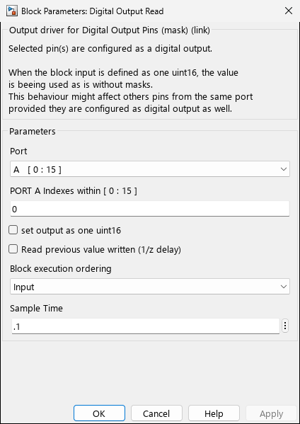
Screenshots taken with chip 33AK512MPS512
Overview
The Digital Output Read block reads the current state of output pins by accessing the LAT (latch) register, not the PORT register. This means it reflects the commanded output value, not the actual pin voltage. Selected pins must already be configured as digital outputs by a Digital Output Write block. The read operation inherently has a 1-sample delay (z^-1) relative to the write, which is useful for diagnostics, state verification, and closed-loop control applications.
When to use:
- Monitoring output states for diagnostics
- Verifying commanded output values
- Implementing closed-loop control with output feedback
- Reading back the state of pins controlled by other blocks
When NOT to use:
- To read external signal levels (use Digital Input instead)
- For immediate feedback without delay (LAT read-back inherently has 1 sample delay)
Block Dialog
No screenshot available — block uses standard parameter dialog similar to Digital Input.
Ports
Output
| Port | Data Type | Description |
|---|---|---|
| Port signal | boolean or uint16 | Current state of LAT register for selected pin(s) with 1 sample delay. If multiple pins are selected without PACK option, each pin has its own boolean output. If PACK option is enabled, a single uint16 output contains LAT states in corresponding bit positions. |
Parameters
| Parameter | Variable | Type | Description |
|---|---|---|---|
| Port | PORT | popup | GPIO port selection (A, B, C, etc.). Dynamically populated based on target device pin map. Shows available pin indices for each port. |
| Pins | PIN | edit | Array of pin indices to read, e.g., [0] or [0 1 2]. Valid range is [0..15] for 16-bit ports or [0..31] for 32-bit ports. Out-of-range or unavailable pins are automatically filtered out with a warning. Pins must be configured as outputs by a Digital Output Write block. |
| set block output as one uint16/uint32 | PACK | checkbox | Conditional. When enabled, returns a single uint16 (16-bit ports) or uint32 (32-bit ports) output where bit positions correspond to pin numbers. When disabled, each pin has an individual boolean output. Always visible. |
| Request exact simultaneous read | SIMULTANEOUS | checkbox | Conditional. When enabled, all pins are read from LAT register in a single access for atomic simultaneous read. Only visible when multiple pins are selected AND PACK is disabled. |
| Block execution ordering | ORDERING | popup | Controls block scheduling: None, Input, Output, or Input & Output. Used for internal ordering in the parent Digital Output subsystem block. |
| Sample Time | SampleTime | edit | Sampling interval in seconds. Use -1 for inherited sample time. |
Device Support
Output Data Type:
- 16-bit ports (dsPIC): PACK mode outputs
uint16, unpacked mode outputs individualbooleanper pin - 32-bit ports (SAM/PIC32A): PACK mode outputs
uint32, unpacked mode outputs individualbooleanper pin
LAT Register Read Behavior:
- This block always reads the LAT register, not the PORT register
- LAT reflects the commanded output value written by Digital Output Write, not the actual pin voltage
- There is an inherent 1-sample delay (z^-1) between write and read-back
- If external circuitry prevents the pin from reaching the commanded voltage (e.g., short circuit, open drain without pull-up), LAT will still show the commanded value
Port Availability:
- The Port popup is dynamically populated from the chip pin map at model initialization
- Only ports with at least one available digital pin are shown
- Pin indices shown in brackets reflect actual chip capabilities
Usage Note:
- This block is typically used as a sub-block within the Digital Output composite block
- It can also be used standalone for diagnostics or to read LAT state of pins controlled elsewhere
- Pins must be configured as outputs (TRIS cleared) for LAT read to be meaningful
Troubleshooting
Problem: Read value doesn’t match expected output
- Solution: Remember that LAT register read-back has a 1-sample delay (z^-1). The value reflects the previously commanded state, not the current external pin voltage.
Problem: Block reads incorrect values
- Solution: Ensure the pins are configured as outputs by a Digital Output Write block elsewhere in the model. LAT register only reflects output state, not input levels.
Problem: Cannot read pin states
- Solution: Verify the pin indices exist on the selected port for your target device. Check that ANSEL configuration doesn’t force pins to analog mode.
Related Blocks
- Digital Output — High-level output block with optional read-back
- Digital Output Write — Write to digital output pins
- Digital Input — Read external digital input signals