TCC PWM


Overview
The TCC PWM block configures the Timer/Counter for Control (TCC) peripheral on SAME5x, SAMC2x, and SAMD2x microcontrollers. TCC modules provide advanced PWM generation with:
- Complementary output pairs (WO0+WO4, WO1+WO5, etc.) with programmable dead-time
- Output matrix (OTMX) to map compare channels (CCx) to waveform outputs (WOx)
- Pattern generator for BLDC motor commutation (hardware-assisted 6-step)
- Recoverable and non-recoverable faults with configurable output states
- Dual-slope (center-aligned) and single-slope (left-aligned) counting
- Dithering for enhanced PWM resolution
- Capture/Compare for position sensing and multi-axis synchronization
The TCC peripheral is optimized for motor control, offering features not available in basic Timer/Counter (TC) modules.
When to use:
- Motor control on SAM E5x, SAM D5x, SAM C2x, or SAM D2x devices
- BLDC commutation with hardware-assisted pattern generation
- Complementary outputs with dead-time for half-bridge/full-bridge drivers
- Applications requiring output matrix flexibility (OTMX) for complex topologies
When NOT to use:
- SAM E7x, SAM S7x, or SAM V7x devices → use PWM SAM7x
- dsPIC devices → use PWM , PWM HighSpeed , or PWM HS FEP
Block Dialog
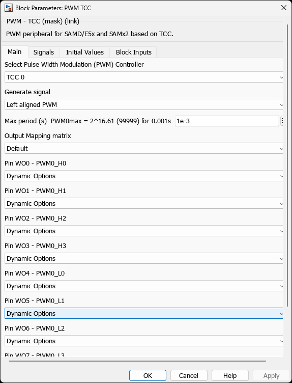
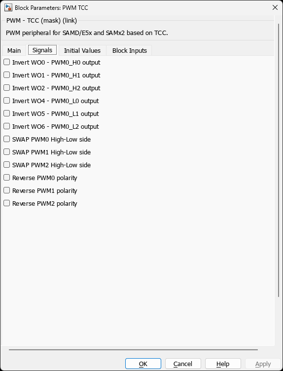
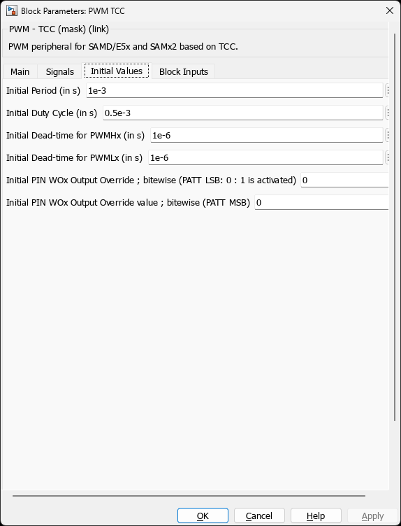
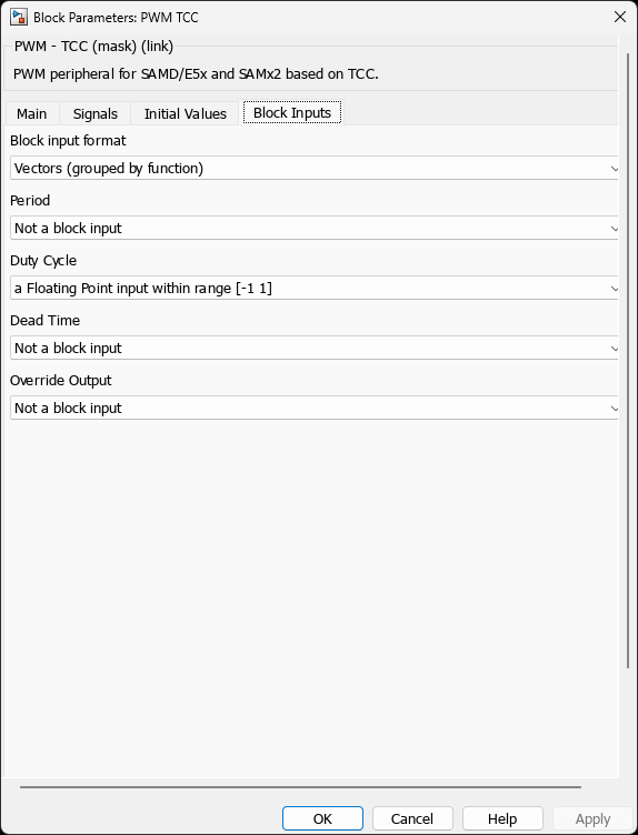
SAME54N20A - TQFP100Ports
Inputs
| Port | Type | Condition | Description |
|---|---|---|---|
| Period | scalar | BlockInput_Period ≠ Not a block input | Updates PERBUF register (synchronized to next period) |
| DutyCycle[N] | scalar or vector | BlockInput_DutyCycle ≠ Not a block input | Updates CCBUFx registers. Vector size = number of enabled channels. |
| DeadTimeH | scalar | BlockInput_DeadTime ≠ Not a block input | Updates WEXCTRL.DTHS (dead-time high-side) |
| DeadTimeL | scalar | BlockInput_DeadTime ≠ Not a block input | Updates WEXCTRL.DTLS (dead-time low-side) |
| Force WOx (PATT reg) | uint16 | BlockInput_OutputOverride = RAW PATT register | Direct write to TCC_PATT or TCC_PATTBUF (bits 0-7: override enable, bits 8-15: output values) |
| Force WOx | uint8 or vector | BlockInput_OutputOverride = Override Activation & pin value | Override enable bitfield (8 bits) |
| Force WOx Value | uint8 or vector | BlockInput_OutputOverride = Override Activation & pin value | Output state bitfield (8 bits) |
| Force WOx | uint8 or vector | BlockInput_OutputOverride = Override Activation only | Override enable only (uses default safe state from InitOutputOverride_val) |
Outputs
The block has no outputs. PWM signals are generated directly on configured WOx pins.
Parameters
Main Tab
| Parameter | Variable | Type | Description |
|---|---|---|---|
| PWM Controller | TCCREF | popup | Select TCC instance: TCC 0, TCC 1, TCC 2, (TCC 3/4 on some devices) |
| Generate signal | WAVE_choice | popup | Left aligned PWM (up counting) or Center aligned PWM (up-down counting) |
| Max period (s) | MaxPeriod_s | scalar | Maximum PWM period. Determines prescaler selection (1/2/4/8/16/64/256/1024) and counter resolution. Workspace variable PWMxmax is created. |
| Output Mapping matrix | OTMX | popup | Selects how Compare Channels (CC0-5) map to Waveform Outputs (WO0-7): Default (WO0→CC0, WO1→CC1, …), Variant 1, Variant 2, Variant 3 |
| Pin WO0..7 | WO0 to WO7 | popup | Assign physical pins to waveform outputs (dynamic per device). Not Used disables that output. |
| Sample Time | SampleTime | scalar | Block execution rate (typically 0.001 for motor control) |
Signals Tab
| Parameter | Variable | Type | Description |
|---|---|---|---|
| Invert WO0..7 output | INVEN_WO0 to INVEN_WO7 | checkbox | Invert output polarity (per WO pin). Applied after dead-time insertion. |
| SWAP PWM0..3 High-Low side | SWAP_PWM0 to SWAP_PWM3 | checkbox | Swap complementary pair assignments (e.g., WO0↔WO4, WO1↔WO5). Useful for PCB layout flexibility. |
| Reverse PWM0..5 polarity | POL_PWM0 to POL_PWM5 | checkbox | Reverse polarity for compare channel output (inverts duty cycle). |
Initial Values Tab
| Parameter | Variable | Type | Description |
|---|---|---|---|
| Initial Period (in s) | InitPeriod_s | scalar | Startup PWM period (PER register value) |
| Initial Duty Cycle (in s) | InitDutyCycle_s | scalar or vector | Duty cycle per enabled channel at startup (CCx register values) |
| Initial Dead-time for PWMHx (in s) | InitDeadTimeH_s | scalar | High-side dead-time (DTHS[7:0], max 255 prescaler ticks) |
| Initial Dead-time for PWMLx (in s) | InitDeadTimeL_s | scalar | Low-side dead-time (DTLS[7:0]) |
| Initial PIN WOx Output Override | InitOutputOverride | scalar or vector | Bitfield: 1=override active for that WO pin (8 bits, one per WO) |
| Initial PIN WOx Output Override value | InitOutputOverride_val | scalar or vector | Bitfield: output state when override active (8 bits) |
Block Inputs Tab
| Parameter | Variable | Type | Description |
|---|---|---|---|
| Block input format | BlockInput_VectorScalar | popup | Independent Scalar (one input per channel) or Vectors (grouped by function) (single vector input) |
| Period | BlockInput_Period | popup | Period input type: Not a block input, Uint raw input, FP [0 1], FP [-1 1], or FP physical scaling (s) |
| Duty Cycle | BlockInput_DutyCycle | popup | Duty cycle input type (same options). If vector mode, one input accepts all enabled channels. |
| Dead Time | BlockInput_DeadTime | popup | Dead-time input type. If enabled, provides separate DeadTimeH/DeadTimeL inputs. |
| Override Output | BlockInput_OutputOverride | popup | Override control mode: Not a block input, RAW PATT register, Override Activation & pin value, Override Activation only. Each mode has (Imm) (immediate) and non-(Imm) (synchronized) variants. |
TCC Instance Availability
| Family | TCC Instances | Channels (CCx) | Outputs (WOx) | Clock Speed |
|---|---|---|---|---|
| SAME54/53/51 | TCC0, TCC1, TCC2, TCC3, TCC4 | 6/4/3/3/2 | 8/4/4/4/4 | 120 MHz |
| SAMC21/20 | TCC0, TCC1, TCC2 | 4/4/2 | 8/4/4 | 48 MHz |
| SAMD51 | TCC0, TCC1, TCC2 | 6/4/3 | 8/4/4 | 120 MHz |
| SAMD21/20 | TCC0, TCC1, TCC2 | 4/2/2 | 8/4/4 | 48 MHz |
Notes:
- TCC0 typically has the most features (6 compare channels, 8 outputs)
- Some devices have additional TCC3/TCC4 with reduced capabilities
- WO outputs are remappable via pin multiplexing (up to 2-4 options per WO)
Output Matrix (OTMX)
The OTMX parameter controls how Compare Channels (CC0-CC5) drive Waveform Outputs (WO0-WO7):
| OTMX | WO0 | WO1 | WO2 | WO3 | WO4 | WO5 | WO6 | WO7 |
|---|---|---|---|---|---|---|---|---|
| Default | CC0 | CC1 | CC2 | CC3 | CC4 | CC5 | CC0 | CC1 |
| Variant 1 | CC0 | CC1 | CC2 | CC0 | CC1 | CC2 | CC0 | CC1 |
| Variant 2 | CC0 | CC0 | CC0 | CC0 | CC0 | CC0 | CC0 | CC0 |
| Variant 3 | CC0 | CC1 | CC1 | CC1 | CC1 | CC1 | CC1 | CC1 |
Usage:
- Default: Standard 6-output motor control (3 complementary pairs)
- Variant 1: Modulo-3 wrapping (for 3-phase systems with fewer CC channels)
- Variant 2: All WO outputs mirror CC0 (synchronized multi-motor control)
- Variant 3: WO0 independent, WO1-7 mirror CC1 (master-slave topology)
Register Configuration (click to expand)
Register Configuration
Initialization (Start function)
// Clock enable (chip-specific GCLK assignment)
GCLK_REGS->GCLK_PCHCTRL[idx_GCLK_PCHCTRLn] = GCLK_PCHCTRL_GEN(GCLK_idx) | GCLK_PCHCTRL_CHEN_Msk;

// Waveform generation mode
TCC_REGS->TCC_WAVE = TCC_WAVE_WAVEGEN_NPWM;      // Left-aligned
                   // or TCC_WAVE_WAVEGEN_DSBOTTOM; // Center-aligned
                   | TCC_WAVE_POLx_Msk;            // Polarity per channel
                   | TCC_WAVE_SWAPx_Msk;           // Swap complementary pairs

// Period and duty cycle
TCC_REGS->TCC_PER = PER_value;
TCC_REGS->TCC_CC[0..N] = CCx_value;

// Dead-time and output matrix
TCC_REGS->TCC_WEXCTRL = TCC_WEXCTRL_OTMX(OTMX)
                      | TCC_WEXCTRL_DTIENx_Msk      // Dead-time enable
                      | TCC_WEXCTRL_DTLS(DTLS)
                      | TCC_WEXCTRL_DTHS(DTHS);

// Output override (pattern generator)
TCC_REGS->TCC_PATT = (override_enable << 0) | (output_value << 8);

// Invert selected outputs
TCC_REGS->TCC_DRVCTRL = TCC_DRVCTRL_INVENx_Msk;

// Start counter
TCC_REGS->TCC_CTRLA = TCC_CTRLA_ENABLE_Msk
                    | TCC_CTRLA_PRESCALER_DIVx
                    | TCC_CTRLA_RUNSTDBY_Msk;
Runtime Updates (Outputs function)
Synchronized Updates (SAME5x/SAMC2x):
TCC_REGS->TCC_PERBUF = new_period;   // Buffered period
TCC_REGS->TCC_CCBUF[x] = new_cc;     // Buffered compare
// Updates applied at next period boundary
Immediate Updates (SAMD2x):
TCC_REGS->TCC_CCB[x] = new_cc;       // Direct compare update
// Takes effect immediately (may cause glitches)
Dead-Time Update:
// Read-modify-write to preserve OTMX and DTIEN settings
tmp_reg = TCC_REGS->TCC_WEXCTRL;
tmp_reg = (tmp_reg & ~TCC_WEXCTRL_DTHS_Msk) | TCC_WEXCTRL_DTHS(new_dths);
tmp_reg = (tmp_reg & ~TCC_WEXCTRL_DTLS_Msk) | TCC_WEXCTRL_DTLS(new_dtls);
TCC_REGS->TCC_WEXCTRL = tmp_reg;
Notes
SAME5x vs SAMD2x Differences
| Feature | SAME5x / SAMC2x | SAMD2x |
|---|---|---|
| Buffered updates | TCC_CCBUF registers (synchronized) | TCC_CCB registers (immediate) |
| Max resolution | 24-bit counter | 24-bit counter |
| Dead-time | 8-bit (DTHS/DTLS) | 8-bit |
| Pattern buffer | TCC_PATTBUF (synchronized) | TCC_PATT (immediate) |
| Fault recovery | Recoverable fault modes | Limited fault support |
Code Generation Adaptation:
The TLC file detects chip family via ::isSAMD2_DA1 flag and generates appropriate register names (TCC_CCB vs TCC_CCBUF).
Dead-Time Limitations
- Dead-time resolution: 8 bits (0-255 prescaler ticks)
- Applied globally to all channels (not per-channel)
- Maximum dead-time depends on prescaler (e.g., 21.3 µs at 120 MHz with DIV1)
- Dead-time is inserted after polarity inversion (INVEN) but before pattern override
Output Override Priority
When pattern generator (PATT register) is active:
- Override replaces PWM generator output
- Dead-time is not applied to overridden outputs
- Polarity inversion (INVEN) is still applied
Safe Override Design:
% Ensure software dead-time in pattern logic
% Bad:  [WO0=1, WO4=1] -> both high-side and low-side ON!
% Good: [WO0=1, WO4=0] or [WO0=0, WO4=1]
Clock Configuration
The block automatically:
- Selects fastest available GCLK (typically GCLK1 @ core frequency)
- Calculates prescaler (1/2/4/8/16/64/256/1024) to fit
MaxPeriod_s - Creates workspace variable
PWMxmax= counter maximum value - Configures
GCLK_PCHCTRLregister for TCC clock routing
Multi-Instance Shared Resources:
All TCC blocks using the same TCCREF must have identical:
MaxPeriod_s(clock prescaler)WAVE_choice(waveform mode)OTMX(output matrix)
Compilation error if mismatch detected via MchpLocal2Global() validation.
Event System Integration
TCC can generate events (via TCC_EVCTRL) for:
- ADC trigger: Synchronize current sampling to PWM valley/peak
- Multi-axis sync: Lock multiple TCC instances to same timebase
- External fault: Connect comparator output to TCC fault input
Example (configured in PWM SAM7x, TCC similar concept):
TCC0_REGS->TCC_EVCTRL |= TCC_EVCTRL_OVFEO_Msk;  // Overflow event
// Route to ADC via EVSYS peripheral
Device Support
- SAM E5x (SAME54P/N/J, SAME53N/J, SAME51N/J 19/20)
- SAM D5x (SAMD51P/N/J/G 19/20)
- SAM C2x (SAMC21N/J/G/E 15/16/17/18)
- SAM D2x (SAMD21G/J/E 15/16/17/18)
Examples
Three-Phase BLDC Motor (SAME54)
% 20 kHz center-aligned PWM with 1 µs dead-time
TCCREF = 'TCC 0';
WAVE_choice = 'Center aligned PWM';
MaxPeriod_s = 1/20e3;  % 50 µs
OTMX = 'Default';

% Pin assignments (3 complementary pairs)
WO0 = 'PA08 / Pin[33]';  % Phase U High
WO4 = 'PA16 / Pin[66]';  % Phase U Low
WO1 = 'PA09 / Pin[34]';  % Phase V High
WO5 = 'PA17 / Pin[67]';  % Phase V Low
WO2 = 'PA10 / Pin[35]';  % Phase W High
WO6 = 'PA18 / Pin[68]';  % Phase W Low

InitPeriod_s = 1/20e3;
InitDutyCycle_s = [25e-6, 25e-6, 25e-6];  % 50% duty
InitDeadTimeH_s = 1e-6;
InitDeadTimeL_s = 1e-6;

% Runtime control
BlockInput_DutyCycle = 'a Floating Point input within range [-1 1]';
BlockInput_VectorScalar = 'Vectors (grouped by function)';

% Connect 3-element duty cycle vector from FOC controller
Synchronized Dual Motor (SAMC21)
% Two motors with phase-locked operation (OTMX Variant 2)
TCCREF = 'TCC 0';
OTMX = 'Variant 2';  % All WO outputs follow CC0

WO0 = 'PA08 / Pin[33]';  % Motor 1 Phase U
WO1 = 'PA09 / Pin[34]';  % Motor 1 Phase V
WO2 = 'PA10 / Pin[35]';  % Motor 1 Phase W
WO4 = 'PA16 / Pin[66]';  % Motor 2 Phase U
WO5 = 'PA17 / Pin[67]';  % Motor 2 Phase V
WO6 = 'PA18 / Pin[68]';  % Motor 2 Phase W

% Single duty cycle input controls both motors identically
BlockInput_DutyCycle = 'a Floating Point input within range [0 1]';
Emergency Shutdown via Override (Immediate)
% Force all outputs LOW on fault (PATT register direct write)
TCCREF = 'TCC 0';
BlockInput_OutputOverride = ' RAW PATT register ; 8 LSB is override active ; 8MSB is out val (Imm)';

% MATLAB Function block:
function patt_reg = shutdown_control(fault)
    if fault
        % Bits 0-7: override enable (all WO outputs)
        % Bits 8-15: output values (all LOW)
        patt_reg = uint16(hex2dec('00FF'));
    else
        patt_reg = uint16(0);  % Normal PWM operation
    end
end
BLDC Commutation with Pattern Generator
% Hardware-assisted 6-step commutation (pattern table in MCU)
TCCREF = 'TCC 0';
BlockInput_OutputOverride = ' Override Activation & pin ouptut value block inputs';

% MATLAB Function for 6-step pattern:
function [override, output] = commutation(hall_state)
    % Hall state 0-7, only 1-6 valid
    patterns = uint8([
        0b00000000;  % Invalid
        0b00100001;  % Hall 1: WO0=1, WO5=1
        0b00001100;  % Hall 2: WO2=1, WO3=1
        0b00101100;  % Hall 3: WO2=1, WO3=1, WO5=1
        0b00110010;  % Hall 4: WO1=1, WO4=1, WO5=1
        0b00110001;  % Hall 5: WO0=1, WO4=1, WO5=1
        0b00011010;  % Hall 6: WO1=1, WO3=1, WO4=1
        0b00000000   % Invalid
    ]);

    override = uint8(63);  % Enable override for WO0-5 (0b00111111)
    output = patterns(hall_state + 1);
end
Programmatic Setup
% Add block to model
add_block('MCHP_Blockset/PWM IO/PWM TCC', [mdl '/TCC_PWM']);

% Configure key parameters
set_param([mdl '/TCC_PWM'], 'TCCREF', 'TCC 0');
set_param([mdl '/TCC_PWM'], 'MaxPeriod_s', '1e-3');
set_param([mdl '/TCC_PWM'], 'InitPeriod_s', '1e-3');
set_param([mdl '/TCC_PWM'], 'InitDutyCycle_s', '0.5e-3');
Related Blocks
- PWM SAM7x — SAM7x PWMC peripheral (higher channel count, more fault options)
- MCHP_ADC_SAM — SAM ADC with TCC event synchronization
- MCHP_QEI_SAM — Quadrature encoder input (Hall sensor interface)
- MCHP_TC_PWM — Basic Timer/Counter PWM (no dead-time, simpler)