Register Access


When to use:
- Tweaking a peripheral register that the standard blocks do not expose (advanced feature, errata work-around, experimental peripheral).
- Reading silicon-specific status or calibration registers during development.
- Custom peripheral bring-up before a dedicated block exists in the library.
- Run-time parameter tuning where a scalar input needs to map directly onto a hardware bit-field.
When NOT to use:
- A dedicated block already exists for the peripheral (use it — the dedicated block handles PPS routing, interrupt declaration, clock dependencies, etc., which Register Access does not).
- Writing to registers that are already owned by another MCHP block in the same model (conflicts are not detected by this block).
- Safety-critical outputs without explicit Saturation on the inputs — Register Access performs no range checking.
Block Dialog
The Register Access block opens a dedicated configuration GUI (launched by double-click) with three sections — Init, Write, Read — and a set of global options.
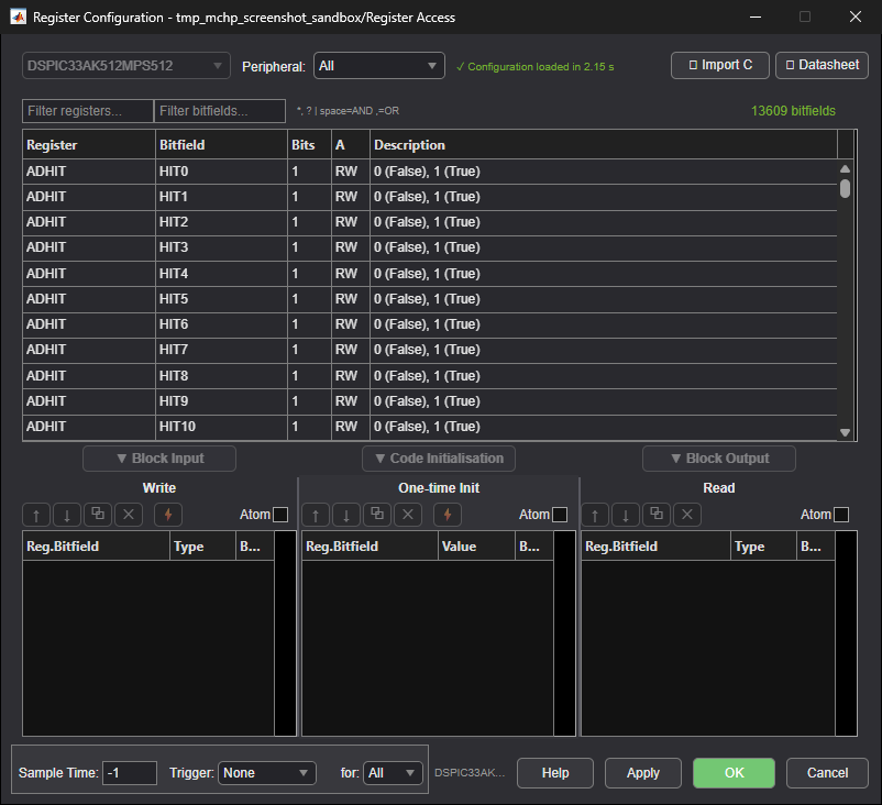
Screenshots taken with chip 33AK512MPS512
Init / Write / Read — what each section does
The Register Access block exposes three independent sections. Each section contains a list of register or bit-field entries; the only difference is when the generated code runs and what direction the data flows.
| Section | Direction | Code emitted in… | When it runs | Simulink ports |
|---|---|---|---|---|
| Init (setup register set) | Constant → Register | <model>_initialize() (the model start function) | Once, at start-up, before the first task tick | None — the value is hard-coded |
| Write | Simulink input → Register | <model>_step() (the task body) | Every task tick (or only when a trigger condition is met) | One input per entry |
| Read | Register → Simulink output | <model>_step() (the task body) | Every task tick (or only when a trigger condition is met) | One output per entry |
Quick mental model
Init = “Configure the peripheral once, then leave it alone.” Typical use: enable a clock, set a PWM polarity bit, write a CRC seed, load a calibration constant.
Write = “Refresh the register every step from a Simulink signal.” Typical use: stream a duty-cycle reference, update a DAC output, push a value computed by the control law into a peripheral.
Read = “Sample a register every step into a Simulink signal.” Typical use: read an ADC result, sample a status flag, capture a timer count for telemetry.
A single Register Access block can mix all three sections — useful when a peripheral needs one-shot setup plus per-step refresh plus per-step status feedback.
Whole register vs single bit-field
Each entry’s Reg.Bitfield column accepts two notations, with significantly different generated code:
| Notation | Effect | Generated code (conceptually) |
|---|---|---|
REGNAME | Operates on the whole register | REGNAME = value; (or value = REGNAME;) |
REGNAME.BITFIELD | Operates on a single field | REGNAMEbits.BITFIELD = value; (or value = REGNAMEbits.BITFIELD;) |
The bit-width and field position are looked up automatically from the on-chip register database — you don’t compute masks or shifts by hand. Changing the chip in the Master block re-validates every entry; entries that don’t exist on the new chip are flagged in red in the GUI.
When to pick which
Bit-field form for the common case: enabling a peripheral, setting a single mode bit, reading one status flag. The compiler emits a read-modify-write that only touches the named field — other fields in the register keep their current value, which is what you almost always want.
Whole-register form for these specific situations:
- You need to assign all fields at once to a known set of values without a read-modify-write (faster; avoids reading the register before writing).
- You’re writing to a write-only register where reading would have side effects.
- You’re writing to a clear-on-write status register (e.g.
IFS0) where you must write a complete word with selected bits set. - You’re reading a register whose only meaningful access is the whole word (e.g.
DEVID).
Rule of thumb: bit-field form by default. Whole-register form when the datasheet explicitly says so, or when you want to skip the read step.
Scaling — float and double inputs/outputs
Most embedded registers are integers, but Simulink control laws often produce floats in physical units (volts, percent, degrees, …). The Scaling option lets you keep the float math in Simulink and have the block convert to the integer representation expected by the register.
How to enable
In the Write or Read row, set Data Type to float or double. As soon as you pick a float type, the GUI shows a scaling editor with two ranges and a live preview graph:
- Input range
[in_min in_max]— the meaningful range of the float signal at the block port - Output range
[out_min out_max]— the integer range as seen at the register
What the codegen actually produces
The TLC computes a gain and offset from the two ranges:
gain   = (out_max - out_min) / (in_max - in_min)
offset = out_min - gain * in_min
and emits, for a Write entry:
REGNAMEbits.BITFIELD = (uint16_T)(gain * float_input + offset); /* clamped if needed */
For a Read entry, the inverse:
float_output = (REGNAMEbits.BITFIELD * (1.0f / gain)) - (offset / gain);
The scaling is fully baked into the constants gain and offset at codegen time — no runtime division and no lookup table, just a multiply-add per converted entry.
Typical mappings
| Use case | Type | Input range (Simulink) | Output range (register) | Effect |
|---|---|---|---|---|
| PWM duty cycle as a percentage | float Write | [0, 100] | [0, 65535] | 0–100 % at the port → 0–65535 raw |
| PWM duty cycle as a ratio | float Write | [0, 1] | [0, 65535] | 0–1 at the port → 0–65535 raw |
| DAC voltage | float Write | [0.0, 3.3] | [0, 4095] | 0–3.3 V at the port → 12-bit DAC code |
| ADC voltage read-back | float Read | [0, 4095] | [0.0, 3.3] | 12-bit ADC code → 0–3.3 V at the port |
| Bidirectional speed reference | float Write | [-1, 1] | [-32768, 32767] | Signed normalised → signed 16-bit |
Scaling gotchas
- Inverted ranges (e.g.
[1, 0]for the input) produce a negative gain — useful for inverting active-low signals, but easy to do by accident. The GUI does not warn about this; double-check the live preview graph. - Out-of-range inputs are not clamped. A float value outside
[in_min in_max]produces an integer value outside[out_min out_max]— and at register-write time the integer is truncated to the bit-field width, which can wrap around silently. Place a Saturation block in front of the Write input if the application requires clamping. - Float resolution. A
float(single-precision) has ~7 decimal digits of mantissa. Mapping[0, 100]to[0, 65535]is fine; mapping[0, 1e6]to a 32-bit register loses precision near the high end. Usedoubleif you need it. - Integer entries are not scaled. If you set Data Type to
uint16(or any other integer type), the scaling fields are hidden — the value goes through as-is.
Atomicity — interrupt-safe operations
By default, the generated code performs each register operation without disabling interrupts. That is fast, but it means an ISR can preempt the block in the middle of a multi-register update.
When to enable atomic
Enable the Atomic checkbox of a section if any of the following is true:
- The section writes two or more registers that the application reads as a coherent set (e.g.
PG1PER+PG1DCupdated on the same step — a partial update would briefly mismatch the period and the duty cycle). - The section reads multiple status registers that change together (e.g. timer high + low halves on a 16-bit chip).
- The same register is written from both the block and an ISR, and the block performs a read-modify-write that the ISR would corrupt.
What the generated code does
When Atomic is enabled on a section, the TLC wraps the entire section in a critical section:
| Architecture | Critical section primitive |
|---|---|
| dsPIC30F / 33F / 33E / 33C (16-bit) | DISICTL / __builtin_disi(N) — disables interrupts for the next N instruction cycles |
| dsPIC33A (32-bit) | __builtin_disable_interrupts() / __builtin_enable_interrupts() |
| PIC32 | __builtin_disable_interrupts() / __builtin_enable_interrupts() |
There are three independent atomic flags — one per section (Init / Write / Read). You usually only need atomicity on the section that contains the multi-register operation; leaving it off on the other sections saves a few cycles per step.
Atomicity gotchas
- DISI countdown limit (16-bit chips): the
DISIinstruction can disable interrupts for at most 16 383 cycles. Very long Write sections may exceed this on classic dsPIC; in that case the codegen splits the section across multiple DISI windows automatically. - Don’t enable Atomic by default. It costs cycles and prevents the scheduler from servicing high-priority ISRs during the protected region. Only enable it where the datasheet, the application, or a trace shows you need it.
Code optimisation — what the block does for you
The Register Access block is not a thin pass-through. The TLC applies several optimisations during code generation. Knowing them helps you predict the resulting code (and lets you exploit them).
1. Per-register read-modify-write coalescing
When multiple bit-fields of the same register are written in the same Write section, the codegen detects this and emits one read-modify-write cycle for the register, not one per field. Internally a temporary union is declared:
typedef union { CCP1CONLBITS bits; uint16_T word; } CCP1CONL_W;
CCP1CONL_W tmpWCCP1CONL;

tmpWCCP1CONL.word     = CCP1CONL;        /* one read */
tmpWCCP1CONL.bits.MOD = 0x4;             /* field 1 */
tmpWCCP1CONL.bits.T32 = 1;               /* field 2 */
CCP1CONL              = tmpWCCP1CONL.word;  /* one write */
This dramatically reduces volatile bus traffic for SFRs that are slow to access (e.g. PIC32 fabric registers).
2. Shared volatile read between Read and Write
If the same register appears in both a Read row and a Write row, the codegen reuses the single volatile read across both — emitting only one fetch of the SFR per step.
3. Compile-time gain/offset folding
Float scaling constants (gain, offset) are evaluated at codegen time and emitted as const literals. There is no runtime division — every Write/Read with scaling is one fused-multiply-add (the FPU instruction on dsPIC33A and PIC32, integer multiply on classic dsPIC).
4. Whole-register fast path
When you use the whole-register notation (REGNAME instead of REGNAME.BITFIELD), the codegen skips the read step entirely — REGNAME = value; is one volatile store, no read.
5. Group-union top placement
The Group union structure on top of the code option lifts all the temporary _W unions to a single declaration block at the top of the function, instead of one declaration per register. Useful when the same Register Access block runs in several tasks of different rates — the unions are shared rather than re-declared.
6. Conditional execution via the Trigger mode
When Trigger Mode ≠ None, the entire Write or Read section (depending on the for selector) is wrapped in an if based on the trigger input — no register access is emitted unless the trigger condition is met. The trigger modes:
| Trigger Mode | Block behaviour |
|---|---|
| None | Section runs every step |
| Level | Section runs while the trigger input is non-zero |
| Rising | Section runs once on each 0 → 1 transition of the trigger input |
| Falling | Section runs once on each 1 → 0 transition |
| Any Edge | Section runs on every transition |
This is faster than wiring an Enabled Subsystem around the Register Access block — there is no subsystem-call overhead.
What the block does not do
- It does not auto-replace single-bit writes with
BSET/BCLRinstructions. If you want guaranteed atomic-bit set/clear, write a one-line C inline-asm via the C Function Call block. - It does not detect cross-block conflicts (another MCHP block writing the same register). Use Port Info for that.
- It does not validate range or saturate float inputs (see the scaling gotchas above).
Parameters
Global Options
| Parameter | Description |
|---|---|
| Chip | Target device (inherited from the Master block; a 16-bit / 32-bit architecture flag is auto-detected and used to size register masks). |
| Trigger Mode | None (every step), Level, Rising, Falling, Any Edge. A trigger mode other than None adds one boolean input port to the block. |
| Trigger applies to | All, Write only, Read only, Init only — selects which section(s) the trigger gates. |
| Init Atomic (DISI) | Wraps the Init section in a critical section. |
| Write Atomic (DISI) | Wraps the Write section in a critical section. |
| Read Atomic (DISI) | Wraps the Read section in a critical section. |
| Sample Time | Period at which the block evaluates. -1 inherits from the parent subsystem. |
Entry Columns
| Column | Description |
|---|---|
| Reg.Bitfield | REGNAME writes the whole register; REGNAME.BITFIELD writes only the specified field (mask and shift are computed automatically). |
| Direction (Write/Read/Init context) | Write (from Simulink input), Read (to Simulink output) or Init (constant). A Write entry with a Literal value produces a constant write with no Simulink port. |
| Type | boolean (1 bit), uint8, uint16, uint32, float, double. float and double enable the scaled conversion described above. |
| Bits | Bit-width of the field (auto-detected; can be overridden). |
| Input / Output Range | [min max] for float entries — used to compute gain and offset at codegen time. |
| Value (Init / Literal only) | Decimal, hex (0xFF), binary (0b1010), an enumeration name from the register database (e.g. 'Primary' for CLKSEL), or a MATLAB workspace variable. |
Advanced Options
| Parameter | Description |
|---|---|
| FLUSH marker | Inserted between rows of the Init or Write section to force the write-back of one register before the next entry runs. Optional delay in clock cycles for peripheral settling. |
| Group union structure on top of the code | Lifts the per-register _W union declarations to the top of the function instead of declaring them inline. |
| Flush GUI | GUI action that re-loads the register list from the current chip (useful after changing the Master block chip). |
| Import C | Imports an existing #define / bit-field configuration block from a .c / .h file as Init entries. |
| Datasheet | Right-click a row and pick Open datasheet to jump straight to the register description in the device datasheet (uses MCHP_Fun.DataSheetLocator). |
Programmatic API
The block can be configured without opening the GUI through the MCHP_Register_API helper class.
cfg = MCHP_Register_API('dsPIC33CK256MP508');     % create config for target chip
cfg.addInit ('PG1CON.ON',         '1');           % one-shot enable
cfg.addWrite('PG1DC',             'uint16');      % per-step duty-cycle from Simulink
cfg.addRead ('PG1STAT.FLTACT',    'boolean');     % per-step fault flag to Simulink
cfg.applyTo('myModel/MCHP_Register');             % push config onto the block
Scaled float entries:
cfg.addWrite('PG1DC',   'float', [0 100]);        % 0–100 % input → 0–65535 register
cfg.addRead ('ADCBUF0', 'float', [0 3.3]);        % 0–4095 register → 0–3.3 V output
Atomicity:
cfg.setWriteAtomic(true); % wrap Write section in DISI
See help MCHP_Register_API for the full method list (addWrite, addWriteLiteral, addRead, addInit, insertFlush, setWriteAtomic, setInitAtomic, setReadAtomic, setTriggerMode, fromBlock, applyTo).
Safety Notes
The Register Access block is a power-user tool and bypasses the safety checks performed by the dedicated peripheral blocks. Pay particular attention to:
- Multi-register atomicity (SAF-004) — Without the Write Atomic option, writes execute sequentially; an interrupt occurring between two writes will see an inconsistent state.
- Input range validation (SAF-001 / SAF-002) — Inverted ranges, negative gains and out-of-range inputs are not validated. Add a Simulink Saturation block in front of each Write input if the application requires clamping.
- Architecture mismatch (SAF-010) — Forcing
archBits = 32on a 16-bit chip is not validated. Keep the chip selection in sync with the Master block. - Cross-block conflicts — If another MCHP block already writes to the same register or bit-field, Register Access will silently overwrite it. Use the Port Info block to audit register and pin assignments.
Examples
Live register tuning (development aid)
Connect a Simulink Constant or a dashboard Slider to a uint16 Write entry targeting a single bit-field (for example PG1DC) and run the model in External Mode: the register value updates on the hardware as soon as the slider is moved, without rebuilding the firmware.
Reading a calibration register
cfg = MCHP_Register_API('dsPIC33AK512MPS506');
cfg.addRead('DEVID',         'uint32');
cfg.addRead('OSCCAL.FRCTUN', 'uint8');
cfg.applyTo('myModel/RegisterRead');
One-shot peripheral bring-up
cfg = MCHP_Register_API('dsPIC33CK256MP508');
cfg.addInit('REFOCONL.ROSEL', 'Primary');     % enum from register DB
cfg.addInit('REFOCONL.ROSLP', '0');
cfg.insertFlush('init', 2, 10);               % 10-cycle settling delay
cfg.addInit('REFOCONL.ROON',  '1');
cfg.applyTo('myModel/RefOscBringUp');
Multi-register atomic update (FOC current loop reference)
cfg = MCHP_Register_API('dsPIC33CK256MP508');
cfg.addWrite('PG1DC',     'float', [-1 1]);   % d-axis duty
cfg.addWrite('PG2DC',     'float', [-1 1]);   % q-axis duty
cfg.addWrite('PG3DC',     'float', [-1 1]);   % zero-axis duty
cfg.setWriteAtomic(true);                     % see all three as one event
cfg.applyTo('myModel/FOC_PWM');
Related Blocks
Port Info — visualize pin and register assignments and detect cross-block conflicts before adding Register Access entries.
Doc — one-click access to the device datasheet and family reference manual.
C Function Call — alternative for inline C code that needs more logic than a register write (e.g. atomic single-bit
BSET/BCLRvia inline asm).Master — required; sets the chip that drives register name resolution.
MCHP_Register_API.m— programmatic configuration helper (inblocks/).help MCHP_Register_API— full method reference.